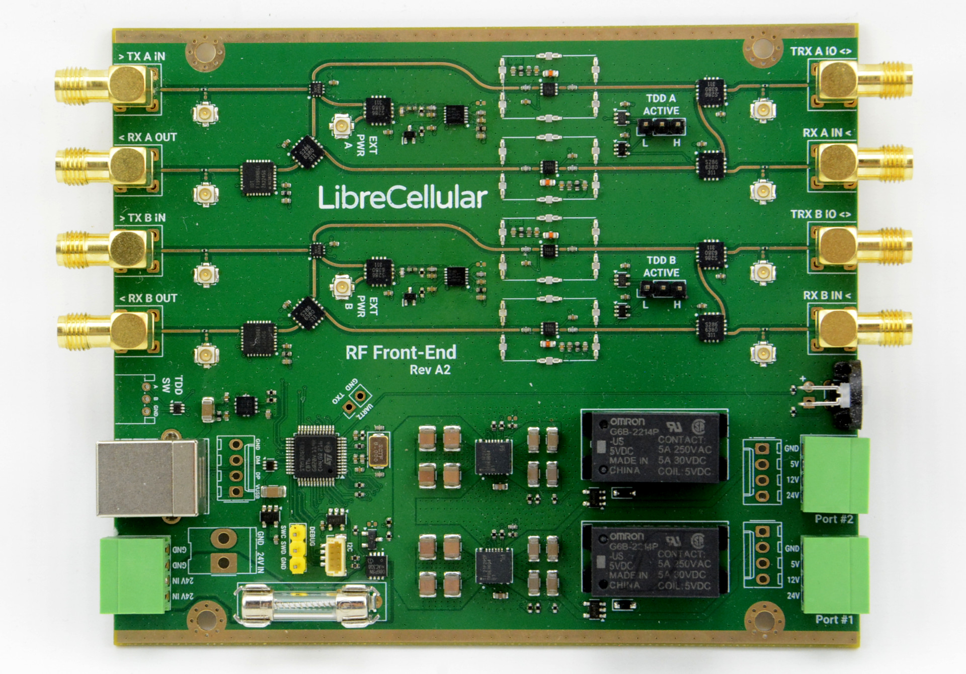
RF Front-End
Software-defined radios tend to provide a very low RF output power and when used to create an LTE base station, this can limit the effective range to a few meters, after which the downlink signal starts to degrade and the available bandwidth is reduced. Furthermore, when using an SDR with a power amplifier it is typically neccessary to use an RF driver stage between the SDR and PA. Meanwhile for anything but close range use, SDRs also benefit from a low noise amplifier (LNA) inserted in the receive path, so as to increase sensitivity in the uplink direction.
The LibreCellular RF Front-End (RFE) provides both downlink and uplink amplification, for configurations up to 2x2 MIMO and with support for both FDD and TDD operation. It also integrates digitally controlled RF step attenuators in the receive path, to enable gain reduction to be set where required.
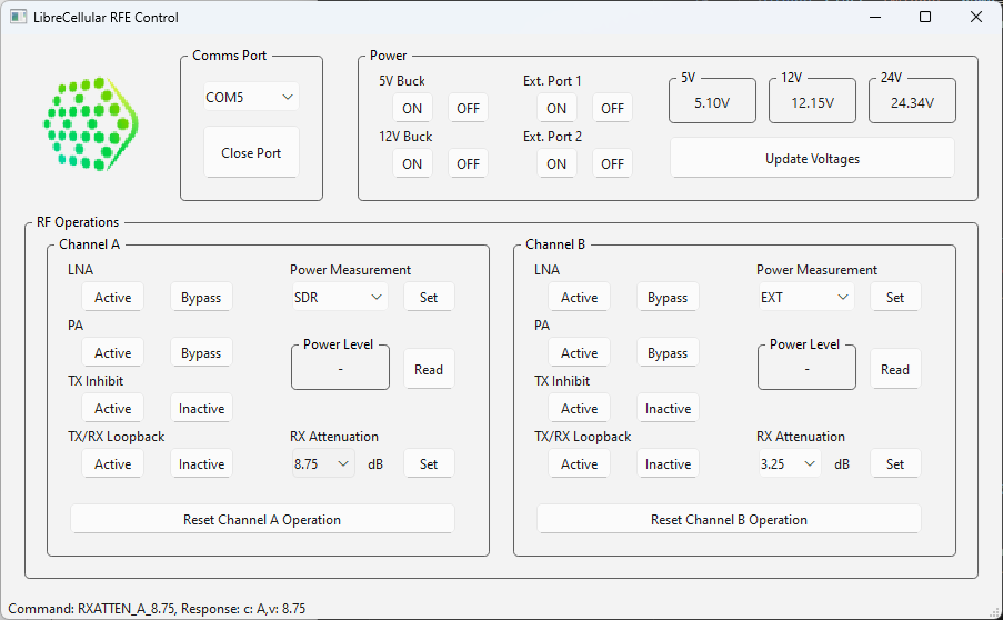
Other useful features include RF power measurement, SDR Tx/Rx loopback, and external PA power sequencing. The RFE uses an STM32 MCU for control and is configured via USB, with a Python GUI for use on the attached host. It also features dedicated inputs for TDD switching, which would typically be connected to an IO pin on the SDR where this mode of operation is used.
For small cell applications the RFE may be used with the addition of only a band-specific duplexer (FDD) or filter (TDD). Where greater coverage is required this may be achieved via the use of RF power amplifiers, with the RFE performing the function of a driver stage and switching DC power to the PAs.
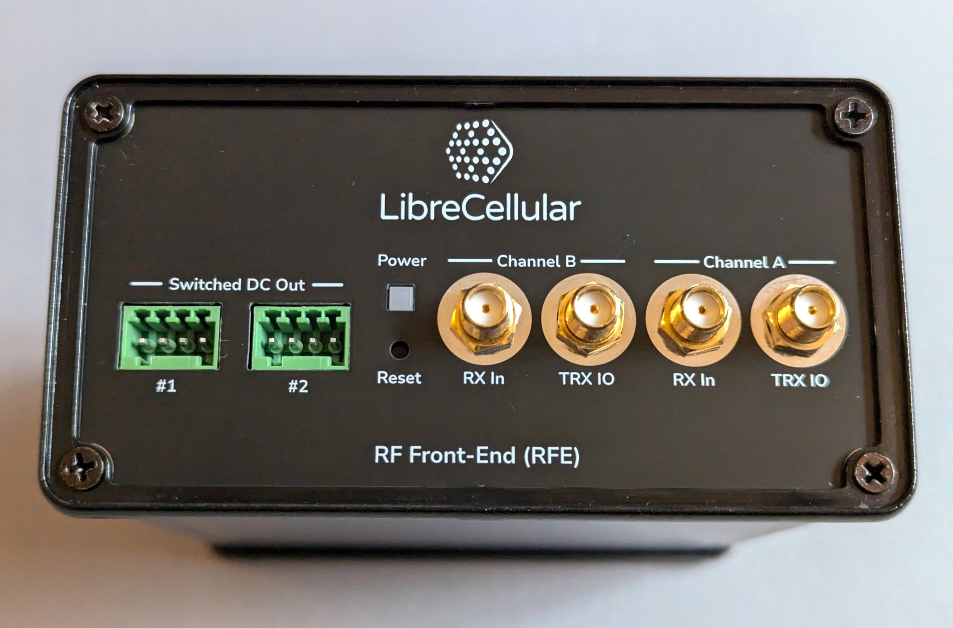
The RFE has been designed so that it can be assembled for either integration into a larger system, such as a base station, or fitting into its own dedicated enclosure for lab use. In the case of the former it is equipped with U.FL connectors, while for standalone use SMA connectors are fitted. Similarly, different connectors for USB, I/O and power are fitted based on usage. In actual fact it may be fitted with both sets of connectors at the same time, but to switch between U.FL and SMA connectors requires 0R resistor links to be changed.
Specifications
MIMO |
2T2R |
Frequency range |
500MHz - 4GHz |
Insertion loss |
TBC |
LNA and PA gain |
19 dB (see below) |
LNA and PA P1dB |
21.2 dBm |
Receive attenuation |
0-31.75 dB |
RF power measurement |
-34 dBm to 6dBm |
Board power supply |
5 VDC (USB 2.0) |
Power supply for switched DC outputs |
12-28V |
Switched DC outputs (per port) |
12-28V (dependent upon input voltage) @ 3A / 12V @ 2A / 5V @ 2A |
Note
Assembled boards have not been fully characterised yet, the gain figure quoted is for the Qorvo TQL9063 part used for the LNA and PA, and there will be insertion loss and likely also reduced performance at higher frequencies due to the use of FR4 PCB substrate in the initial design.
Theory of operation
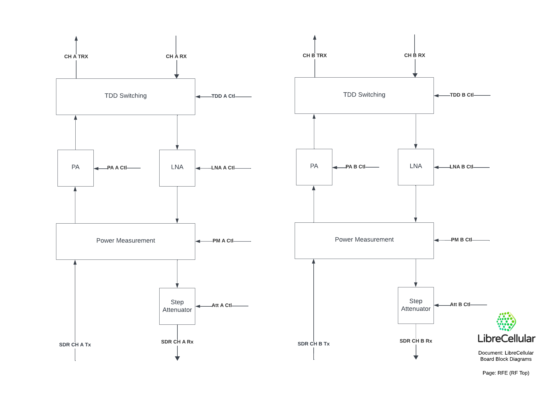
The RFE is comprised of two identical channels, A and B, each with transmit and receive branches.
The RF drivers, LNAs and RF step attenuation may all be bypassed and are by default, and are controlled by an STM32 MCU which features a USB interface.
The transmit signal from the SDR (downlink) is routed via an RF power measurement block to an RF driver. Following which the transmit signal is routed via TDD switching to the TRX out port.
The receive signal input (uplink) is first routed via the TDD switching block to an LNA. Following which the receive signal is routed via the power measurement block, and a programmable RF step attenuator, and finally on to the SDR.
By default the transmit signal input is routed to the corresponding TRX out port. Similarly the receive signal input is routed to the corresponding RX out port. However, when the TDD line is toggled, the transmit signal is terminated by an absorbtive RF switch and the TRX port is connected to the receive branch. Hence with TDD operation the TRX port is used for both transmit and receive, with switching typically controlled by an attached SDR. The RFE has been designed to support the fast switching times required by TDD operation in mobile networks.
Note
The TDD switching inputs are unused with FDD operation.
TDD may also be made active via USB control, so as to provide a simple transmit inhibit function. This is useful with SDRs which emit an unwanted signal when calibration is run prior to streaming starting, as this may be activated before the eNodeB starts and then made inactive once it is running. Thereby preventing unwanted signals from being radiated.
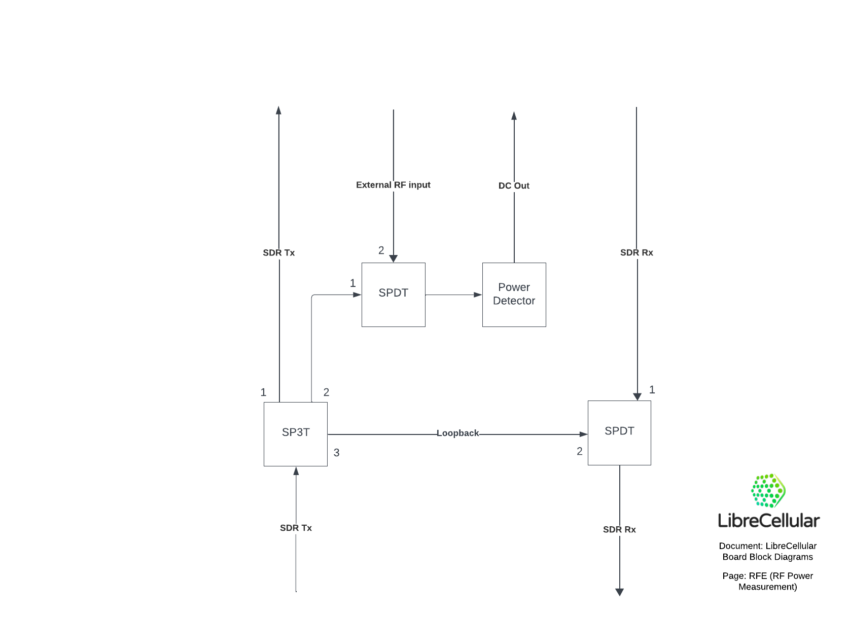
The RF power measurement block is bypassed by default. In SDR mode it is configured to measure the SDR transmit power output. Once this is known the block may then be configured to provide Tx/Rx loopback and following which the SDR RSSI function may be calibrated.
The block may also be set to EXT mode to measure the RF power of an external signal input on a UFL connector. This would typically be connected to a directional coupler located after any downstream RF amplification, thereby enabling the final downlink transmit output power to be measured.
Note
External RF input is only available on a U.FL connector, as it is assumed that this would generally be used when the RFE is integrated into a larger system.
Design
The PCB design has been entered using KiCAD and for details, see the RFE Hardware GitHub repository.
Firmware & Software
For the RFE control firmware and software see the RFE Control GitHub repository.
Credits
LibreCellular RFE schematic capture, board layout, firmware and software development by Ordinatra Minima.