LTE Band 3 Medium Power Amplifier
Low power RF amplifiers for cellular bands can be obtained as off-the-shelf items without too great a cost. Whereas amplifiers which are capable of producing a few watts or more of RF power tend to become quite expensive. Meanwhile the advent of spectrum licensing schemes which permit operation of medium power systems — such as Ofcom Shared Access in rural designated areas — has meant that affordable medium power RF amplifier solutions are needed.
The objective is to create a low cost RF power amplifier for LTE Band 3 (1800 MHz), which can be used together with another amplifier as a driver stage, between the SDR and the final PA. A target minimum modulated power output of 32dBm (1.6W) has been set, which into an 8dBi gain antenna would result in an EIRP of 40dBM (10W).
Note
Modern wireless systems such as LTE use waveforms which have a high Peak-to-Average Power Ratio (PAPR), which means that a power amplifier back-off of 7-10dB is typically required in order to maintain linearity in the PA. This is essential for ensuring both good system performance and wireless regulatory compliance.
Version 1.0
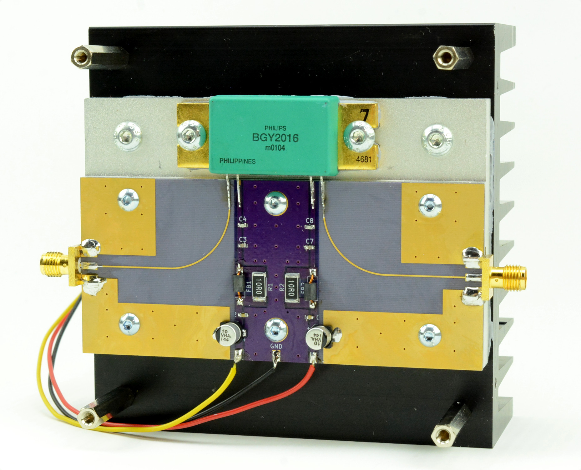
The initial design makes use of a BGY2016 three-stage UHF amplifier module, which is specified to have a gain of at least 28dB and a CW (not modulated) output power of 16W. The reason for selecting this particular device is that, while it is not a current part, it is available in large numbers via sites such as AliExpress and can cost as little as around £8 in single quantity.
Design

B3 MPA v0.1 schematic diagram.
The BGY2016 data sheet provides a reference layout for fabrication using a high performance PCB laminate which is commonly used in professional RF designs. However, since this is quite expensive, the design has been modified to use the OSH Park 4-layer Prototype Service (FR408-HR substrate), which is much lower cost and has previously been used with good results in a number of RF designs.
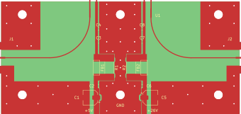
B3 MPA v0.1 PCB layout.
Warning
The design should not be fabricated using a regular 2 layer PCB service, since this will not provide sufficient impedance control. Other appropriate substrates could be used, however, the microstrip traces would need to be recalculated and modified accordingly.
The PCB design was entered using KiCAD. The project files have been published to the lc-b3-mpa repository. This repository also includes the mechanical design for a CNC machined aluminium palette, which is used to thermally couple the RF module to a heatsink. The palette design also assumes a board fabricated using the OSH Park 4-layer substrate and similarly may need to be modified if some other stack-up were used.
Bill of Materials
Component |
Description |
Manufacturer |
Man. Part |
Distributor |
Dist. Part |
|---|---|---|---|---|---|
U1 |
UHF Amplifier |
Philips |
BGY2016 |
||
J1-2 |
Board edge mount SMA connector |
Wurth Elektronik |
60312202114514 |
RS Components |
|
C4,8 |
10pF MLCC capacitor |
AVX |
06035A100KAT2A |
RS Components |
|
C3,7 |
100pF MLCC capacitor |
AVX |
06031A101JAT2A |
RS Components |
|
R1-2 |
10Ω 1W 2512 SMD resistor |
KOA |
RK73HW3ATTE10R0F |
RS Components |
|
FB1-2 |
Grade 4S2 ferrite bead |
Ferroxcube |
BD3/1/4-4S2 |
Farnell |
|
C2,6 |
10nF MLCC capacitor |
Kemet |
C0603C103J5RACTU |
RS Components |
|
C1,5 |
10uF SMD electrolytic capacitor |
Panasonic |
EEEHA1V100R |
RS Components |
|
Misc |
0.5mm enamelled wire |